GATE DELAYS
A delay, as used in Verilog, is a number of time units it takes to receive a response of a circuit. In a simple forward combinational circuit this is a time it takes to obtain a change on an output when an input is altered.
Let's say a synchronous circuit is triggered by a positive clock transition; `the delay' is then the time it takes for the circuit to change its outputs from the time the clock line is set high rather then a time it takes to change the outputs since data lines altered.
Types of delays
There are three basic types of delay which can be used:
The time it takes to set an output high (trise); this applies to a transition which may start from any (`0', `1', `X' or `Z') state
The time it takes to set an output low (tfall); similarly, applies to transitions which begin in any state and finally, the time it takes to cut-off a buffer (toff). Syntax gate with delay:
gate_type#(t_rise, t_fall, t_off) instance_name (output_port,input_port1, input_port2,...);
For example:
and #(1, 3) g1 (o1, i1, i2);
nor #(2) g2 (o2, i3, i4);
The above parameters are specified in sequence and if a cut-off time is to be specified the fall time cannot be omitted. One more interesting transition is a move of an input from a defined logic state i.e. either `0' or `1' to an `X' (don't care). In such case, the shortest of the two times t fall, trise is used. For an inverse case (`X'->`0'|`1') the longer delay is used.
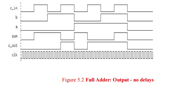
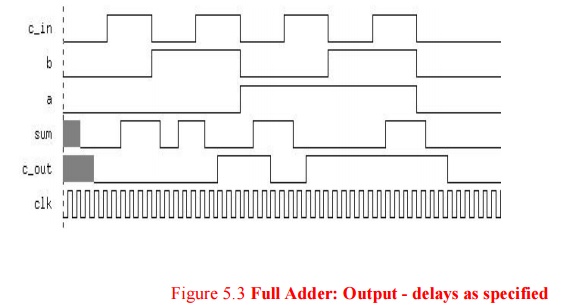
Example: Single bit full-adder
The design below is for a full adder, written using gate-level modelling techniques. A gate-level model of a 1-bit full-adder:
modulefull_adder(sum, c_out, a, b, c_in);
outputc_out, sum; input a, b, c_in; wire p, q, r;
xor #(3,2) x0 (p, a, b);
xor #(3,2) x1 (sum, p, c_in);
and #(2,4) a0 (q, a, b); and #(2,4) a1 (r, p, c_in); or #(3) o0 (c_out, q, r);
end module