
LOGICAL EFFORT
Logical effort is a gate delay model that takes transistor sizes into account. Allows us to optimize transistor sizes over combinational networks. Isn’t as accurate for circuits with reconvergentfanout.
1. Logical effort gate delay model
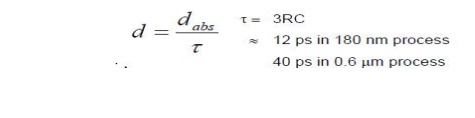
Express delays in process-independent unit
Gate delay is measured in units of minimum-size
Inverter delay τ
Gate delay formula:
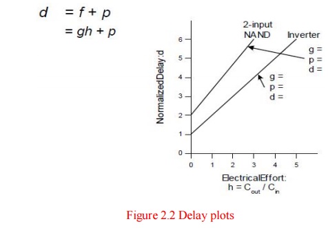
d = f + p.
Effort delay f is related to gate’s load. Parasitic delay p depends on gate’s structure. Represents delay of gate driving no load set by internal parasitic capacitance
2. Effort delay
Effort delay has two components: f = gh.
Electrical effort h is determined by gate’s load: h = Cout/Cin Sometimes called fanout
Logical effort g is determined by gate’s structure. Measures relative ability of gate to deliver
current g ≡ 1 for inverter
3. Delay plots
4. Computing Logical Effort
Logical effort is the ratio of the input capacitance of a gate to the input capacitance of an inverter delivering the same output current. Measure from delay vs. fanout plots Or estimate by counting transistor widths