SCALING
In scaling there are really two issues
• Devices Can we build smaller devices
· What will their performance be try to avoid the wet noodle effect Wires
· There is concern about our ability to scale both of these Components
1. Limitations
Limitations to device scaling has been around since working in 3m nMOS, 22 years ago (actually bipolar)
• Worries were
§ Short channel effect
§ Punchthrough
• drain control of current rather than gate
§ Hot electrons
§ Parasitic resistances
• Now worries are a little different
§ Oxide tunnel currents
§ Punchthrough
§ Parameter control
§ Parasitic resistances
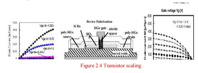
2. Transistor scaling
People are building very short channel devices
§ Shown are I-V curves for 15nm L pMOS
§ And a short channel nMOS
§ The structure is strange
§ FinFET
But you can make them work
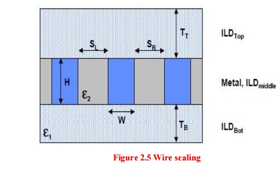
3. Wire scaling
More uncertainty than transistor scaling
§ Many options with complex trade-offs
• For each metal layer
§ Need to set H, TT, TB, e1, e2, conductivity of the metal