
1 Memory Organization
ü Logical separation of program and data memory
ü Separate address spaces for Program (ROM) and Data (RAM) Memory
ü Allow Data Memory to be accessed by 8-bit addresses quickly and manipulated by 8-bit CPU
Program Memory
ü Only be read, not written to
ü The address space is 16-bit, so maximum of 64K bytes
ü Up to 4K bytes can be on-chip (internal) of 8051 core
ü PSEN (Program Store Enable) is used for access to external Program Memory
Data Memory
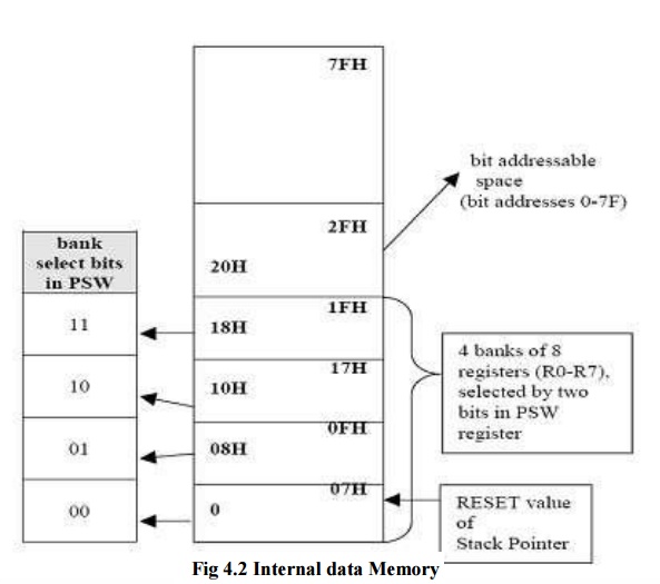
ü Includes 128 bytes of on-chip Data Memory which are more easily accessible directly by its instructions
ü There is also a number of Special Function Registers (SFRs)
ü Internal Data Memory contains four banks of eight registers and a special 32- byte long segment which is bit addressable by 8051 bit-instructions
ü External memory of maximum 64K bytes is accessible by “movx”
2 Interrupt Structure
ü The 8051 provides 4 interrupt sources
ü Two external interrupts
ü Two timer interrupts
3 Port Structure
ü The 8051 contains four I/O ports
ü All four ports are bidirectional
ü Each port has SFR (Special Function Registers P0 through P3) which works like a latch, an output driver and an input buffer
ü Both output driver and input buffer of Port 0 and output driver of Port 2 are used for accessing external memory
ü Accessing external memory works like this
ü Port 0 outputs the low byte of external memory address (which is time- multiplexed with the byte being written or read)
ü Port 2 outputs the high byte (only needed when the address is 16 bits wide)
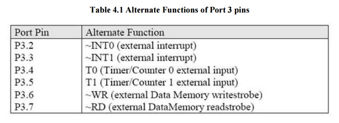
ü Port 3 pins are multifunctional
ü The alternate functions are activated with the 1 written in the corresponding bit in the port SFR
Table 4.1 Alternate Functions of Port 3 pins
4 Timer/Counter
ü The 8051 has two 16-bit Timer/Counter registers
1. Timer 0
2. Timer 1
ü Both can work either as timers or event counters
ü Both have four different operating modes