The MOS technology lies in the limited load driving capabilities of MOS transistors. This is due to the limited current sourcing and current sinking abilities associated with both p- and n- transistors.
Bipolar transistors provide higher gain and have generally better noise and high frequency characteristics than MOS transistors and have effective way of speeding up VLSI circuits.
When considering CMOS technology, there is difficulty in extending the fabrication processes to include bipolar as well as MOS transistors.
Indeed, a problem of p-well and n-well CMOS processing is that parasitic bipolar transistors are formed as part of the outcome of fabrication.
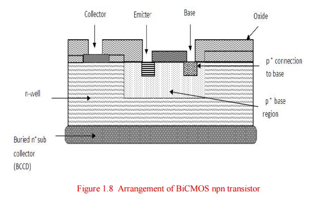
The production of npn bipolar transistors with good performance characteristics can be achieved by extending the standard n-well CMOS processing to include further masks to add two additional layers such as the n+subcollector and p+ base layers.
The npn transistors is formed in an n- well and the additional p+ base region is located in the well to form the p-base region of the transistor.
The second additional layer, the buried n+subcollector (BCCD), is added to reduce the n-well (collector) resistance and thus improve the quality of the bipolar transistor. The arrangement of BiCMOS npn transistor is shown in Fig. 1.8.
There are several advantages if the properties of CMOS and bipolar technologies could be combined. This is achieved to a significant extent in the BiCMOS technology.
A further advantage which arises from BiCMOS technology is that analog amplifier design is facilitated and improved
High impedance CMOS transistors may be used for the input circuitry while the remaining stages and output drivers are realized using bipolar transistors.
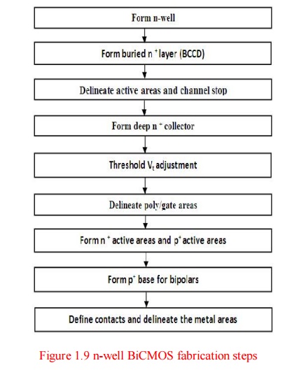
Since extra design and processing steps are involved as in Fig. 1.10, there is an increase in cost and some loss of packing density.